Prototyping Techniques
When producing electronics for the laboratory, we often need to only make a few copies of our circuit, making manufacturing on a commercial scale unreasonable. There are a number of prototyping techniques that can be used to create circuits that are semi-permanent or permanent. We will cover the basics of each technique and its unique advantages/disadvantages.
Breadboard
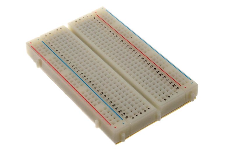
The breadboard is the most versatile way to prototype electronics. A perforated plastic grid covers copper spring contacts. Components and wires can be pushed into the holes and the spring contacts make a good, but temporary electrical connection. Breadboards commonly contain power busses for convenience. Generally the vertical rows on each side of the center are electrically connected. Breadboards are useful for the initial prototyping of circuits when the design is being tested and iterated on often. This type of construction is also useful for temporary or demonstration circuit construction.
There is some stray capacitance introduced into your circuit when using a breadboard. Long component legs and any flying jumper wires can be places for interference to be radiated/received. Breadboards are not suitable for radio frequency (RF) prototyping, but are often adequate for laboratory circuits. There are products on the market that are placed on top of the breadboard before the circuit is built and allow you to later remove the components and solder them to a permanent board. This is suitable for basic circuits with a careful initial circuit layout.
The video below demonstrates the capacitance effect of a breadboard:
Perf/Vero Board
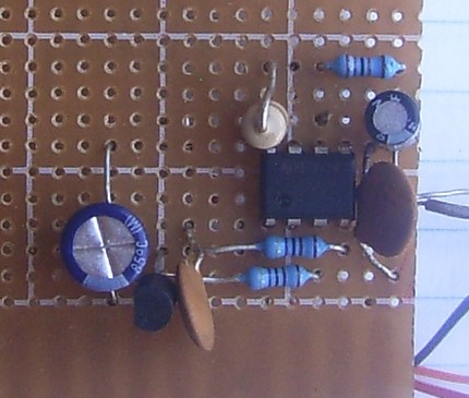
Perf-board or vero-board can be used to create more permanent versions of circuits. These boards are made of an insulating material with a grid of holes drilled in it. Some designs have no copper pads or electrical connections, but many have pads to allow easy soldering and mechanical securing of the components. Different designs are available with connection patterns between rows and columns of holes to aid circuit construction with fewer jumpers.
This prototyping technique has many of the same issues as breadboard prototyping, but is a more permanent construction technique and one of the most popular. Some technicians prefer to use a tool to cut copper traces on the bottom of the boards to further increase the number of connections that can be made without jumpers. Layout of these prototypes requires some planning, but can make very nice low to mid-frequency circuits.
Manhattan
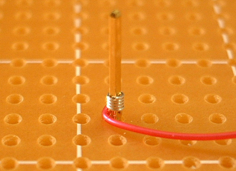
Manhattan prototyping is commonly used for high frequency and RF circuit prototyping and construction. A copper clad board is used as a ground plane and islands are cut or glued on to provide common connection points for components. Components are often wired in the air even. Keeping leads short is important! This construction can look messy, but when done well is an art. There are products available (like this kit ) that provide glue on solder pads of various size and footprint, but often scrap bits of copper clad are used. Another way to create connection islands is with a hollow drill, such as this one.
This technique is named for the skyscraper/skyline look of the components standing up off the board. When integrated circuits are used, they are often glued to the board upside down with their pins facing upward. This is referred to as dead bug construction. This technique is very good at high frequencies, but can produce a slightly fragile circuit, so an enclosure is recommended.
Wire-Wrap
Wire-wrap uses special wire and a tool to strip, and firmly mechanically bond the wire to a square post with sharp corners. Wire wrapping is often used to prototype digital circuits in a semi-permanent way. Modifying wire wrap boards can become time consuming when many wires are connected to a single post or there are many overlapping wires. Special sockets for parts are required for this technique, but it can be a fast way to prototype and was often used in the design of early computers.
Wire wrapped designs are good for relatively high speed circuits, but not useable for modern computing speeds or often for low noise analog designs.
Quick-turn PCB
In the last few years it has become economical to design a custom printed circuit board (PCB) and have it manufactured. Traditionally, you needed to produce a large number of boards to work with a manufacturer and the designs were made with cut tape patterns, called “taping out” a board. Now, computer design tools make laying out a board a relatively simple process. PCBs can be created with copper connections on a single side, on both sides, or even with many layers of copper sandwiched in between layers of insulators. Signals are passed between layers with holes that are copper plated called vias.
PCBs, when designed correctly, can be used for very high frequency and low noise designs. Laying out a circuit board takes considerable time, so that should be considered before setting out in this direction. The price with panel-sharing services such as OSH Park can be as low as $5/sq-in for a double sided board. Designs are generally made in a few days, but overnight manufacturing can often be arranged for a significant fee. Be sure to check the design rules for your manufacturer and set your CAD tool to enforce them to ensure a working board!
Examples
This video by Alan Wolke shows many excellent examples of the various electronics prototyping techniques and is packed full of great resources.